

Apex industry body Indian Electrical & Electronics Manufacturers’ Association (IEEMA) has welcomed the positive step by the Union Cabinet to clear the Production Linked Incentive (PLI) Scheme for semiconductors.
“This is a huge positive step for the Indian Electrical & Electronics industry. I believe this will accelerate our indigenization efforts and enable global competitiveness of our industry to ramp-up exports of finished products”, said Vipul Ray, President, IEEMA.
Ray hailed it as one of the most significant moves towards realizing the vision of AatmNirbhar Bharat; one which has come at an opportune time to tackle the global shortage of semiconductors. “It should help streamline the disrupted global supply chain and help mitigate the cyber security risks”, he added.
“Semiconductors are widely used in manufacturing of many electrical equipments like smart energy meters, control & automation products, testing & measurement Instruments and switching products, to name a few. Electrical and allied industry will be hugely benefited by smooth and competitive supply of semiconductors within the country once fab facilities are established. This will also enhance our export competitiveness” Ray added.
High level of sophistication
Manufacturing processes of Semiconductors require sophisticated equipment demanding huge investments. The proposed incentives worth Rs 76,000 crore, over the next six years and the provision for 25 per cent incentives on capital expenditure for establishing unit of compound semiconductor wafer fabrication, assembly, testing, and packaging facility in the country will encourage the manufacturing industry, apart from bringing investments and employment in the country and savings of foreign exchange, a release from IEEMA said.
Background
To position India as the global hub for Electronic System Design and Manufacturing (ESDM), the Union Cabinet chaired by Prime Minister Narendra Modi, on December 15, 2021, approved the comprehensive program for the development of sustainable semiconductor and display ecosystem in the country. The scheme has an outlay of Rs.76,000 crore.
The program will usher in a new era in electronics manufacturing by providing a globally competitive incentive package to companies in semiconductors and display manufacturing as well as design. This shall pave the way for India’s technological leadership in these areas of strategic importance and economic self-reliance.
Foundation of modern electronics
Semiconductors and displays are the foundation of modern electronics driving the next phase of digital transformation under Industry 4.0. Semiconductors and display manufacturing is very complex and technology-intensive sector involving huge capital investments, high risk, long gestation and payback periods, and rapid changes in technology, which require significant and sustained investments. The program will give an impetus to semiconductor and display manufacturing by facilitating capital support and technological collaborations.
The programme aims to provide attractive incentive support to companies engaged in
- Silicon Semiconductor fabs
- Display fabs
- Compound Semiconductors / Silicon Photonics / Sensors (including MEMS) fabs, Semiconductor Packaging (ATMP / OSAT)
- Semiconductor Design
Fiscal support
The scheme for setting up of semiconductor fabs and display fabs in India shall extend fiscal support of up to 50 per cent of project cost on pari passu basis to applicants who are found eligible and have the technology as well as capacity to execute such highly capital intensive and resource incentive projects.
Government of India will work closely with the state governments establish high-tech clusters with requisite infrastructure in terms of land, semiconductor grade water, high quality power, logistics and research ecosystem to approve applications for setting up at least two greenfield semiconductor fabs and two display fabs in the country.
Semiconductor Laboratory
Union Cabinet has also approved that Ministry of Electronics and Information Technology will take requisite steps for modernization and commercialization of Semiconductor Laboratory (SCL). MeitY will explore the possibility for the Joint Venture of SCL with a commercial fab partner to modernize the brownfield fab facility.
Also read: IEEMA T&D Conclave Focuses On Smart Technologies
Multiplier Effect
Development of semiconductor and display ecosystem will have a multiplier effect across different sectors of the economy with deeper integration to the global value chain. The program will promote higher domestic value addition in electronics manufacturing and will contribute significantly to achieving a $1 trillion digital economy and a country with a $5-trillion GDP by 2025.
Comprehensive Fiscal Support
Inclusive of the PLI scheme for semiconductors, the government of India has committed support of Rs.2,30,000 crore to position India as global hub for electronics manufacturing with semiconductors as the foundational building block.
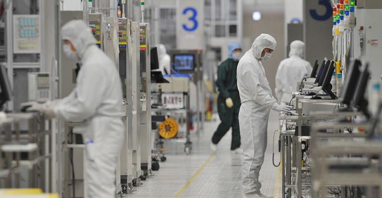
Featured photograph (source: datacenterknowledge.com) is for representation only